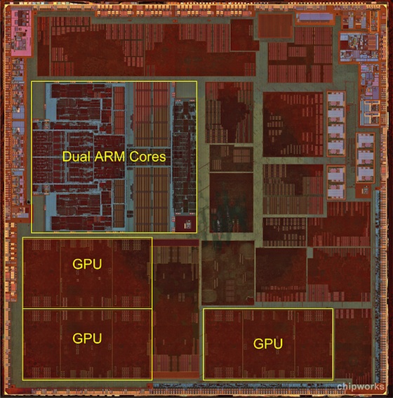
iFixit and Chipworks have partnered on a teardown of the A6 system-on-a-chip, Apple’s custom design that powers the iPhone 5. While several of the high-level details such as 1 GB of RAM and a dual-core CPU paired with triple-core graphics have already been shared, the teardown confirms all of these details with high-resolution images showing the various components of the chip.
Perhaps most notably, the custom ARM-based CPU developed by Apple for the A6 appears to have been manually laid out on the die, an expensive and time-consuming process but one that can offer greater efficiency than automatic layout.- When compared to the rigid, efficient layout of the GPU cores directly below it, the layout of the ARM cores looks a little homespun—at first.
– Generally, logic blocks are automagically laid out with the use of advanced computer software. However, it looks like the ARM core blocks were laid out manually—as in, by hand.
– A manual layout will usually result in faster processing speeds, but it is much more expensive and time consuming.
– The manual layout of the ARM processors lends much credence to the rumor that Apple designed a custom processor of the same caliber as the all-new Cortex-A15, and it just might be the only manual layout in a chip to hit the market in several years.
The report also takes a look into the die, where it confirms that the A6 is manufactured using Samsung’s 32-nanometer HKMG process that was trialled earlier this year with the A5 that made its way into the third-generation Apple TV and the revised iPad 2.
Finally, iFixit and Chipworks took a look at a number of other chips from the iPhone 5, sharing die photos from Qualcomm’s MDM9615M modem and RTR8600 RF transceiver, a Cirrus Logic audio amplifier chip, and Murata’s Wi-Fi/Bluetooth module incorporating a chip from Broadcom with other components.